 |
| October 04, 2016 | Volume 12 Issue 37 |
Designfax weekly eMagazine

Archives
Partners
Manufacturing Center
Product Spotlight
Modern Applications News
Metalworking Ideas For
Today's Job Shops
Tooling and Production
Strategies for large
metalworking plants
Blazingly fast chips ease congested battlefield operations
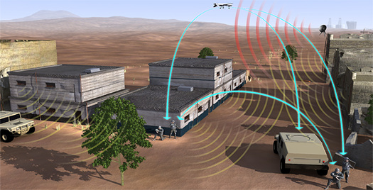
With the help of innovative new chips that can convert analog radar and other electromagnetic signals into digital data that can be processed at unprecedented speeds, warfighters can look forward to enhanced situational awareness in the midst of battle.
Competition for scarce electromagnetic (EM) spectrum is increasing, driven by a growing military and civilian demand for connected devices. As the spectrum becomes more congested, the Department of Defense (DoD) needs better tools for managing the EM environment and for avoiding interference from competing signals.
One recent advance, an exceptionally high-speed analog-to-digital converter (ADC), represents a major step forward. Funded by the Defense Advanced Research Projects Agency (DARPA), the ADC could help ensure the uninterrupted operation of spectrum-dependent military capabilities, including communications and radar, in contested EM environments.
The advance was enabled by 32-nm silicon-on-insulator (SOI) semiconductor technologies available through DARPA's ongoing partnership with GlobalFoundries, a manufacturer of highly advanced semiconductor chips. The EM spectrum, whose component energy waves include trillionth-of-a-meter-wavelength gamma rays to multi-kilometer-wavelength radio waves, is an inherently physical phenomenon. ADCs convert physical data -- that is, analog data -- on the spectrum into numbers that a digital computer can analyze and manipulate, an important capability for understanding and adapting to dynamic EM environments.
Today's ADCs, however, only process data within a limited portion of the spectrum at a given time. As a result, they can temporarily overlook critical information about radar, jamming, communications, and other potentially problematic EM signals.
DARPA's Arrays at Commercial Timescales (ACT) program addressed this challenge by supporting the development of an ADC with a processing speed nearly 10 times that of commercially available, state-of-the-art alternatives. By leveraging this increased speed, the resulting ADC can analyze data from across a much wider spectrum range, allowing DoD systems to better operate in congested spectrum bands and to more rapidly react to spectrum-based threats.
How fast is fast? The new ADC samples and digitizes spectrum signals at a rate of over 60 billion times per second (60 GigaSamples/sec). That's fast enough to directly detect and analyze any signal at 30 GHz or below -- a range that encompasses the vast majority of operating frequencies of interest. Whereas scanning through these frequencies today requires costly application-specific hardware with long development cycles, the new ADC can provide a "one-stop shop" for processing radar, communications, and electronic warfare signals.
As desirable as these blazing sampling speeds are, they also pose challenges. The amount of data generated is staggering, reaching nearly a terabyte per second. This high data rate requires on-chip data-management circuitry that allows signals to be processed locally on the ADC, reducing the amount of data that must be communicated to neighboring electronics. This on-board digital signal processing burns quite a bit of power and also demands state-of-the-art transistors. The 32-nm SOI technology offered by Global Foundries, the only certified DoD supplier of this circuit technology, provided ACT with the leading-edge transistors needed to sample and process the RF spectrum without exceeding power or data-transfer limitations.
Upcoming ACT designs will go further. By using GlobalFoundries' even more advanced 14-nm technology, ACT's next generation of ADCs aims to reduce power requirements by an additional 50 percent and enable even smaller and lighter systems that can sample even greater swaths of the spectrum.
These ongoing improvements in semiconductor-based components highlight the benefit of DARPA's longstanding commercial partnerships with players who have mastered the upper limits of modern transistor technology, said Troy Olsson, manager of the ACT programs. "Our performers combined innovative designs with advanced fabrication facilities and techniques to create world-class technology," Olsson said. "And we are already seeing exciting results that closely match our design expectations."
Source: DARPA
Published September 2016
Rate this article
View our terms of use and privacy policy